This is a revised version of an article first published in the journal Nanomaterials.
Think of solar energy and you will most likely picture in your mind panels fixed to the roofs of buildings that lap up the sun’s rays on fair weather days, and do nothing much at all when the skies are overcast. Readers familiar with developments in nanoscience and technology may also consider organic thin-film photovoltaics that promise to be cheap to produce and have wide application.
Photovoltaics are typically designed to capture visible and ultraviolet light from our neighbourhood star, and turn this abundant, carbon-free energy into electricity. But what of all the indirect solar energy in the form of heat reflected and radiated from buildings, including at night when the sun doesn’t shine? And not only solar energy: there is much heat generated by machinery and electronic devices that might be recycled. Rather than let it go to waste, could this mid-infrared thermal energy be captured and made use of?
The answer to this question is yes. Or at least it is in principle. Back in 2001, University of South Florida chemical engineer Yogi Goswami, who is co-director of the Clean Energy Research Center, delivered a keynote lecture at the Solar Energy Congress in Adelaide, Australia. In his presentation Goswami highlighted three new and emerging technologies, and flagged infrared energy collection as one to look out for. Not only was the conversion of solar energy in electromagnetic field form feasible, he said, the technology had enormous commercialisation potential.
“It’s just a matter of time before somebody comes up with something they can demonstrate working, and has the efficiency that you need,” says Goswami. “And, if that happens, cost will not be a problem.” Especially if you can print the antennas on cheap, flexible substrates, he adds.
In terms of concept, the capture of infrared radiation by electromagnetic antennas is not new. The basic principles were first suggested in 1972 by University of Florida engineer Robert Bailey, who in the following year, with his NASA colleague JC Fletcher, published a technical outline and was awarded a US patent. The only problem was that in the early 1970s the technologies did not exist to make solar energy antennas work. It was an idea ahead of its time.
Three and a half decades later, based on what researchers at the Idaho National Laboratory (INL) presented to the 2008 International Conference on Energy Sustainability in Jacksonville, Florida, this is no longer the case.

Idaho scientists Steven Novack and Dale Kotter, MicroContinuum CTO Dennis Slafer and University of Missouri engineer Patrick Pinhero announced at the Jacksonville meeting that they have developed sheets of infrared nanoantennas which could power everything from hybrid cars to MP3 players with an efficiency exceeding that of traditional solar cells. A number of other research groups are rumoured to be working on similar technologies, but they have not gone public owing to the commercial potential of their work, says Goswami.
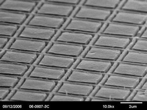
The nanoantennas created by Novack and his colleagues are tiny gold square-edged spirals set in a specially treated polyethylene film. Various metals including gold, manganese and copper were investigated, and their behaviour at the terahertz frequencies associated with infrared radiation modelled. The researchers found that with gold structures of a certain shape and size, their computer-simulated nanoantennas could harvest up to 92% of incident infrared radiation.

“We started our modelling using analytical tools to get a ballpark design,” says Kotter. “Then we validated it with some code from Ohio State University called ‘periodic method of moments’, which is based on algorithms developed to support military applications. That code did not account for all the material properties we encountered at thermal wavelengths, so we modified the method of moments with some proprietary algorithms that we have a patent pending on.”
And the extremely high frequencies involved are critical, explains Novack: “One of the challenges for the modelling is that analytical data for the response of materials – specifically metals – at these high frequencies are not available. Secondly, codes that incorporate the responses of these materials at these high frequencies were not developed. So we had to develop the code, and then use analytical methods to gather the high-frequency responses of these materials.”
Armed with the model outputs, the team then built some prototype antennas. They first etched a silicon wafer with the modelled nanoantenna pattern, and found that the silicon-based antennas matched the computer simulations, absorbing more than 80% of incident infrared energy over the desired wavelength range. Following this the researchers used a stamp and repeat process to emboss their gold spiral nanoantennas on thin sheets of plastic. Tests show that the performance of these plastic-based antennas also matches theoretical predictions.

Building an antenna to capture infrared radiation is one thing, but converting alternating currents oscillating at terahertz frequencies to the direct current required for energy storage and use is quite another. Apart from a small number of experimental devices, today’s rectifiers simply cannot handle terahertz frequencies without significant energy loss.
One potential solution is to embed a rectifier diode into the antenna structure, and in their conference presentation the researchers spoke of metal-insulator-insulator-metal tunnelling diodes as a possibility. MIIM diodes consist of a thin barrier layer and two dielectric oxide layers sandwiched between metal electrodes with different amounts of energy required to remove electrons from their surfaces. With a large enough electric field present, electrons can tunnel across the barrier layer, and the difference in work function between the metal junctions produces non-linear effects which result in high-speed rectification.
“There has been a lot of work done in this area, and people are making progress,” says Novack. “We’ve seen progress over the last year, close to the frequencies we’re interested in. Theoretically, the results are showing us that it can be done, but there’s still probably three to four years of research that needs doing before we can get circuits we think are going to get us reasonable efficiencies. We have some ideas on the designs; we’re not letting those out yet, but are exploring them with different partners.”
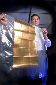
Now that they have succeeded in using a stamp and repeat process to emboss gold nanoantennas on plastic, the next step for the researchers is to make rolls out of the master templates. “As the plastics come through the rolls they would be stamped, and then we would have deposition of the antenna metal structures onto those formations inside the plastics,’ says Novack. ‘Stamp and repeat is a precursor to roll-to-roll processing.”
As for bringing the technology to market, this will depend on how successful the researchers are in implementing the electronics into the stamp and repeat process. “The major difficulty in laying down the electronics is that we have multiple layers, and that’s going to complicate our process slightly,” says Novack. “When we look at the designs of some of the circuitry we’re going to put in there, we’re going to have to very closely align with the processes we’ve already come up with. This is going to take a little longer to develop.”
Novack and his colleagues may have made significant progress in antenna fabrication, but Goswami stresses that this is a known technology. “In the chip industry they have the feature size an order of magnitude less than what has been done in this work,” he says. “Although for this concept they have shown it to work, I’m not going to say that they are the first, because I know of others who have also done it but are not publishing.”
The key to enabling this infrared solar energy technology is the diode. Not just producing the device, but making it efficient enough to be viable. You could gather as much as 90% of the incident radiation with an antenna, but still this has to go through some kind of diode. “If the diode efficiency is only 1%, then what you’ve got is 0.9% overall efficiency,” says Goswami. “But if the diode efficiency is, say, 50%, then you’ve got around 45% overall efficiency, and that is tremendous!”
If Novack’s group, or any others working in this field, can achieve an overall efficiency in their antennas and electronics of 50%, and keep the cost down to an order of magnitude less than conventional semiconductor-based photovoltaics, then the technology will take off and create a whole new renewable energy industry.
In the meantime there are, says Novack, some intermediate applications for both passive and semi-active antenna structures: “We’re planning on proceeding along with some of those things we’ve already accomplished – to modify designs both environmentally and structurally to support these different applications before we get to energy storage or energy use.” Examples of such intermediate applications include building insulation, window coatings and heat dissipation in consumer electronic products.
The technical challenges may be considerable, but Goswami is optimistic. “I’m bullish on it, as I was in 2001 when I gave that lecture,” he says. “I feel very confident that this will eventually be on the market.”
Further reading
“New and emerging developments in solar energy”, Goswami et al., Solar Energy 76, 33 (2004).
“A proposed new concept for a solar energy convertor”, RL Bailey, J. Eng. Power 94, 73 (1972)
“Electromagnetic wave energy convertor”, JC Fletcher and RL Bailey, US Patent No. 3 760 257
Figures
(1) An array of loop nanoantennas, imprinted on plastic and imaged with a scanning electron microscope. The deposited wire is roughly 200 nanometers thick (source: Idaho National Laboratory).
(2) A flexible panel of interconnected nanoantennas may one day replace heavy, expensive solar panels. Each square contains roughly 260 million antennae (source: Idaho National Laboratory).
(3) Idaho National Laboratory researcher Steven Novack holds a plastic sheet containing nanoantenna arrays created by embossing the antenna structure and depositing a conductive metal in the pattern. The INL-patented manufacturing process could be adapted to a large-scale roll-to-roll process akin to newspaper presses (source: Idaho National Laboratory).